
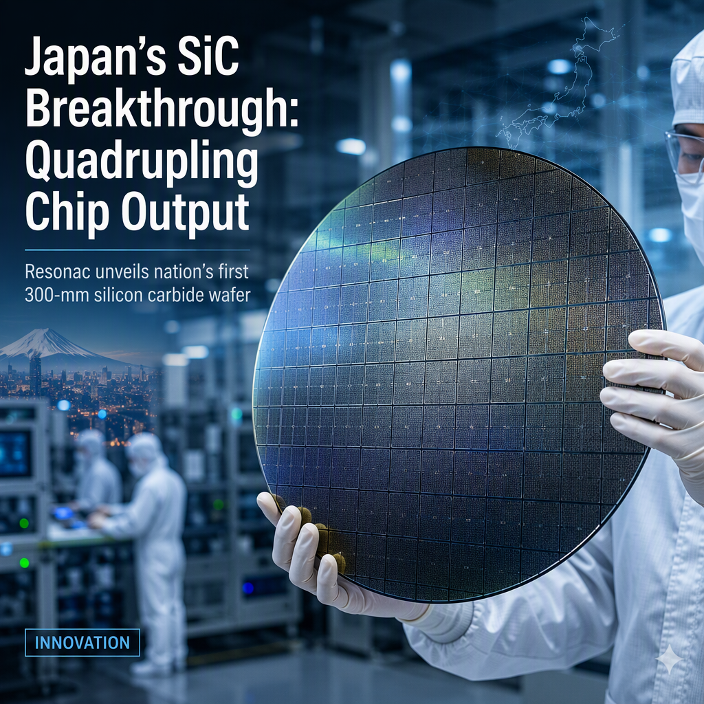
Resonac Holdings has announced the development of Japan's first 300-mm silicon carbide (SiC) substrate, marking a significant technological breakthrough in the semiconductor industry [1]. This new wafer size enables the production of up to four times as many integrated circuits compared to the current industry-standard SiC substrates, which are typically 150-mm or 200-mm in diameter [1]. The larger surface area of the 300-mm wafer allows for simultaneous manufacturing of more chips per wafer, which is expected to boost productivity and reduce the cost per chip [1].
This development positions Resonac alongside U.S. and Chinese competitors who are also working on large-diameter SiC substrates, but commercial production of such wafers has not yet been realized by any company [1]. The innovation is particularly timely as demand for power semiconductors is rising, driven by the growth of electric vehicles (EVs) and renewable energy applications, where SiC chips are valued for their efficiency and heat resistance [1].
Resonac's achievement is anticipated to strengthen Japan's role in the global semiconductor supply chain and could provide Japanese manufacturers with a competitive edge if commercialization and adoption proceed as expected [1]. However, the company has not disclosed any details regarding commercial production timelines or pricing, and ongoing research and development will focus on improving yield rates and overcoming technical challenges before mass production can begin [1].
CONCLUSION
Resonac's development of a 300-mm SiC wafer represents a major step forward for Japan's semiconductor industry, with the potential to significantly increase chip output and reduce costs. While commercial production details remain undisclosed, this innovation could enhance Japan's competitiveness in the global market, especially as demand for power semiconductors continues to grow.