
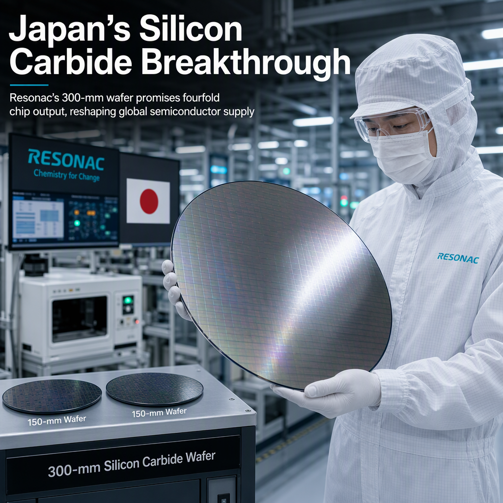
Resonac Holdings has announced the development of Japan's first 300-mm silicon carbide (SiC) substrate, marking a significant technological milestone in the semiconductor industry [1]. This new substrate can yield four times as many integrated circuits compared to the current standard substrates, which are typically 150 mm or smaller [1]. The larger wafer size is expected to substantially boost chip production yields, particularly for power electronics and advanced semiconductor applications [1].
Resonac's achievement places it alongside U.S. and Chinese competitors who have also been working to commercialize 300-mm SiC substrates [1]. The increased output per wafer could help meet the rising global demand for power semiconductors, especially in sectors such as electric vehicles, renewable energy, and industrial automation [1]. Market analysts suggest that the ability to mass-produce these larger wafers could lower the production cost per chip and enhance profitability for device manufacturers [1].
Industry observers are closely monitoring Resonac for further details regarding commercialization timelines, production yields, and potential partnerships with semiconductor device makers [1]. The company's advancement is seen as a strategic move to strengthen its competitive position in the global semiconductor materials market [1].
CONCLUSION
Resonac's development of a 300-mm SiC substrate represents a major leap forward for Japan's semiconductor industry, potentially reshaping the competitive landscape. The innovation is expected to drive higher chip yields and lower costs, with significant implications for power semiconductor supply chains. Market participants are awaiting further updates on commercialization and industry collaborations.